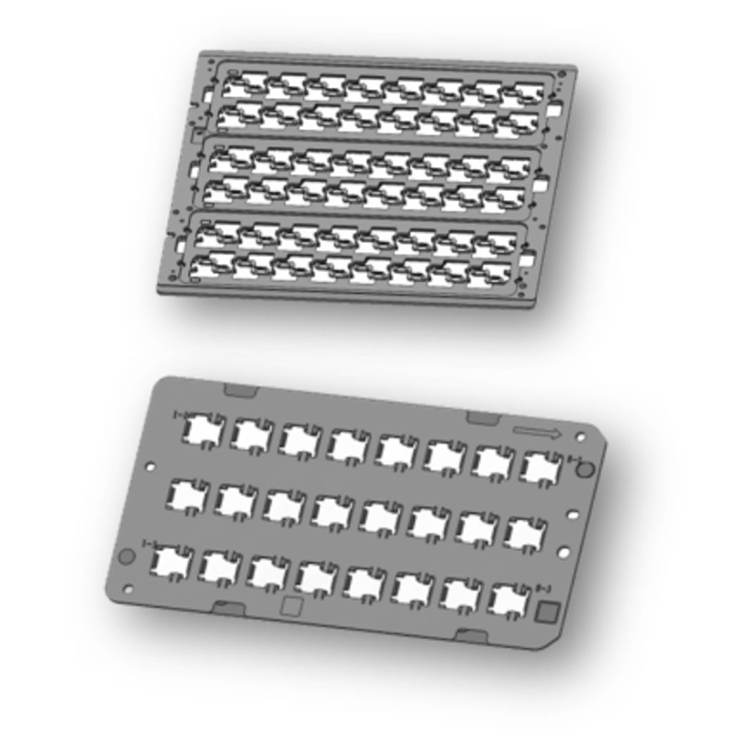
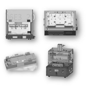
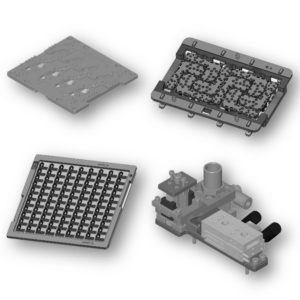
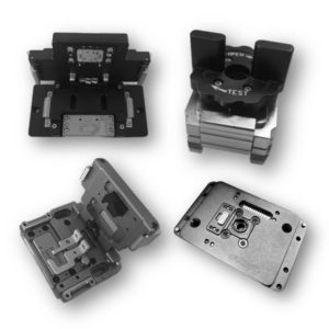
◆ The processing technology is complex and the processing accuracy is high: the dimensional accuracy of the cavity is ≤ 0.02mm, and the flatness is ≤ 0.05mm
◆ Processing stress requirement: The flatness change before and after overall baking and heating (230 ℃/2.5 hours) should not exceed 50um
Platform contact heating (175 ℃/60 seconds), the flatness change of the cover plate under heating state is not more than 50um
◆ Use magnetic materials and high temperature resistant magnets to achieve the fitting of the upper and lower covers
◆ High load-bearing accuracy and good stability
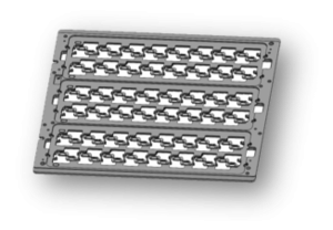
(SMT Carrier)
◆ The processing technology is complex and the processing accuracy is high: the cavity size accuracy is ≤0.02 mm , and the flatness is ≤0.05 mm
◆ High bearing accuracy and good stability
APPLICATION:
The 3C industry (mobile phones, wearables, tablets, laptops) carries components such as cameras or displays with PCBA attached